With the rapid development of IoT smart devices, embedded systems, and automotive electronics, the demand for highly reliable, low-power, and fast-response storage solutions is growing. The W25Q128JVSIQ, a high-performance SPI NOR flash memory chip from Winbond’s W25Q series, stands out with its 128Mbit capacity, industrial-grade wide temperature support, and high-speed QSPI interface. It is widely adopted in smart homes, wearables, industrial sensors, and other low-power IoT terminals, delivering fast boot and stable data performance.
At the same time, the W25Q128JVSIQ also meets the stringent reliability and latency requirements of automotive ECUs, dashboards, infotainment, and ADAS systems. With features such as XIP (Execute-In-Place) and OTA firmware update support, it enables secure performance upgrades and flexible design iteration. This article will explore the chip’s technical specifications, key applications, advantages in IoT and automotive systems, and migration considerations for selecting compatible alternatives.
1. What is the W25Q128JVSIQ?
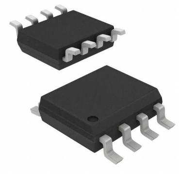
The W25Q128JVSIQ is a high-performance SPI NOR flash memory chip manufactured by Winbond Electronics. It features a compact SOIC-8 package design with 8 integrated pins. This chip supports an industrial-grade operating temperature range (-40°C to 85°C) and a power supply voltage of 2.7V to 3.6V, enabling stable operation in various embedded systems and IoT devices. The W25Q128JVSIQ supports the standard SPI protocol and dual/quad I/O SPI modes, and is compatible with XIP (Execute-In-Place) functionality. It can transmit data quickly at SPI clock speeds up to 133 MHz, making it suitable for devices requiring fast response and stable storage.
2. W25Q128JVSIQ Technical Specifications
| Feature | Specification |
|---|---|
| Storage Capacity | 128 Mbit (approx. 16 MB) |
| Data Interface | SPI bus; supports Dual and Quad I/O, QPI high-speed mode |
| Package Type | 8-pin SOIC (surface mount) |
| Supply Voltage | 2.7V to 3.6V (single supply) |
| Maximum Clock Frequency | 133 MHz |
| Operating Temperature | -40°C to 85°C (industrial range) |
| Memory Organization | Optional: 4,096 × 4KB sectors or 65,536 × 256B programmable pages |
| Manufacturing Process | Winbond 58nm process |
Note: For complete technical information or pin definitions, please visit the Winbond official datasheet or authorized distributors (such as DigiKey, Mouser Electronics, Findchips).
3. Main Applications of the W25Q128JVSIQ Chip
Consumer Electronics and Networking Devices
The W25Q128JVSIQ is widely used in consumer electronics and network communication devices for storing system boot code, firmware, applications, and multimedia resources.
Consumer Electronics Applications
It serves as secondary storage in smart devices such as smartphones and tablets. It is also commonly used as boot firmware memory in digital cameras, and as a caching solution for UI resources in smart TVs.
Printer & Office Equipment
In printer motherboards, such as some Epson models, the W25Q128JVSIQ stores system firmware and configuration data to ensure reliable operation and fast system updates.
Networking & Communication Devices
For routers, switches, modems, and communication modules, this SPI NOR flash memory can store device configurations, operational logs, and upgradeable firmware. This enhances stability, improves recovery capabilities, and supports long-term maintenance.
Optimized for IoT Devices
Leveraging high read/write speeds and low latency characteristics, the W25Q128JVSIQ enables fast system boot, real-time responses, and efficient over-the-air (OTA) updates, making it ideal for connected IoT applications.
Embedded Systems, IoT, and Automotive Control
- Embedded Systems and IoT Devices: The W25Q128JVSIQ provides reliable support for firmware storage, sensor data logging, and OTA (Over-The-Air) firmware updates. Its 128Mbit capacity and 4KB sector management mechanism are suitable for storing master firmware and periodic log data, while facilitating differential or sector-level OTA updates, reducing flash memory write operations and extending lifespan. For battery-powered IoT devices, the chip’s low-power mode and deep power-down capabilities help extend device battery life.
- Automotive and Industrial Control Systems: The W25Q128JVSIQ’s industrial-grade temperature range (-40°C to 85°C) and high durability make it suitable for critical units such as ECUs, infotainment systems, dashboards, and sensor gateways for storing boot codes, calibration parameters, and safety-related data. Because automotive applications have higher requirements for data integrity and product lifecycle, selection should simultaneously evaluate indicators such as write/erase life, data retention time, and automotive-grade certifications (e.g., AEC-Q100). Computer peripherals (keyboards, mice, external storage controllers, etc.) also frequently utilize this chip to store firmware and personalized configuration data for rapid recovery and upgrades.
- Computer peripherals: Used in devices such as keyboards, mice, and hard drives to store firmware and configuration data.
The W25Q128JVSIQ supports four-channel SPI/QPI (Quad SPI/QPI), providing fast read channels at high frequencies. Combined with XIP (Execute-In-Place) functionality, it allows the processor to execute code directly from flash memory without copying the entire program to RAM, thus shortening boot time and reducing RAM requirements. This feature is particularly advantageous in memory-constrained MCUs and IoT devices, significantly reducing BOM costs and improving user experience. Combined with OTA update strategies, developers can implement remote firmware replacement and rollback mechanisms, while strengthening firmware security through the chip’s write protection and unique ID functions.
4. Technical Advantages of the W25Q128JVSIQ in IoT and Automotive Systems
Application Advantages in IoT Devices
- Low Power Design: Leveraging IoT flash memory chip technology, the W25Q128JVSIQ supports a deep power-down mode of 1µA, making it ideal for battery-powered wearables, smart sensors, and portable terminals, significantly extending actual battery life.
- Fast Boot and XIP Support: Through a QSPI interface up to 133 MHz, the host MCU can directly run code from flash memory using XIP (Execute-In-Place), enabling smart home and edge computing devices to achieve shorter boot times and more stable response performance.
- Firmware Storage and Data Logging: 128Mbit capacity is sufficient for application firmware, runtime logs, and multi-sensor data storage; simultaneously, the 4KB sector erase structure makes OTA firmware updates more flexible and less power-consuming, suitable for large-scale IoT terminal deployments.
- Firmware Security Mechanism: The chip incorporates a unique 64-bit ID and provides hardware locking and software write protection, effectively reducing the risk of firmware copying, replacement, or tampering, thus enhancing data security for IoT devices.
- Compact Packaging: Offers compact packaging options such as SOIC-8, facilitating board layout in confined spaces and making it suitable for hardware designs in wearable devices, micro-sensors, and lightweight smart terminals.
Application Advantages in Automotive Systems
AEC-Q100 Automotive-Grade Reliability: The automotive-grade version of the W25Q128JVSIQ complies with the AEC-Q100 standard, maintaining stability under prolonged vibration, high temperatures, and electrical noise, making it suitable for ECUs and vehicle controllers.
Wide Operating Temperature Range: Supports an industrial-grade operating range of -40°C to 85°C, with some automotive-grade models extending to 125°C, allowing safe deployment in extreme environments such as engine compartments and high-power control modules.
- Critical Boot Code Storage: Widely used in digital dashboards, ADAS (Advanced Driver Assistance Systems), and infotainment systems to store sensitive boot code, system firmware, and calibration parameters, ensuring reliable power-on of vehicle systems.
- Functional Safety and Lifecycle Management: Supports flash memory solutions compliant with ISO 26262, offering stable write/erase life and data retention capabilities, contributing to improved vehicle functional safety and long-term operational reliability.
- Graphics Rendering and High-Speed Response: Leveraging the high-speed QSPI interface, it enables faster graphics loading and interface switching in applications such as automotive infotainment screens and dashboards, enhancing the driving experience and system real-time performance.
Through these technological advantages, the W25Q128JVSIQ achieves a balance of high reliability, high performance, and low power consumption in IoT smart devices and automotive electronics, helping engineers and developers optimize product design and system performance.
5. W25Q128JVSIQ Alternatives and IoT Flash Memory Chip Compatibility
The W25Q128JVSIQ is a mid-capacity member of the Winbond W25Q series. This series maintains a high degree of consistency in instruction sets (standard SPI NOR instruction set / JEDEC compliant instructions) and basic timings, meaning that models such as the W25Q128JVSIQ, W25Q64, and W25Q256 are directly compatible at the software level in most designs, requiring no significant modifications to read/write instructions. For IoT designs requiring capacity upgrades or downgrades (e.g., from 64Mbit to 128Mbit), engineers can typically replace the chip without changing the MCU driver logic, thereby accelerating product iteration cycles and reducing firmware adaptation costs.
Tip (Design Check): When replacing, timing parameters, maximum clock frequency, and deep power-down characteristics should still be checked to ensure that the new model operates stably under the target controller frequency and power supply conditions.
When considering alternatives to the W25Q128JVSIQ, refer to compatible devices on the market such as the GigaDevice GD25Q128, Macronix MX25L128, and ISSI (e.g., IS25LP128). These products are generally consistent with or highly compatible with the W25Q series in terms of instruction set and functionality, but differences exist in electrical characteristics (Vcc range), erase/write life, read speed, and protection mechanisms. The datasheet should be consulted for selection. For IoT products or industrial applications, prioritize comparing the following parameters: rated voltage range (2.7–3.6V), maximum CLK frequency (e.g., 133MHz QSPI), deep power-down current, erase/write/program latency, and data retention years.
Regarding packaging, the W25Q series offers various packages including SOIC-8, WSON-8 (USON), and BGA/DFN. If the project requires direct replacement of the capacity model without changing the PCB, ensure that the pinout of the new device is consistent with the original package. Different packages have significant differences in pad size, thermal characteristics, and maintainability; production and testing feasibility should be considered simultaneously during the design phase. Replacing from DIP/SOIC to WSON may require adjustments to the PCB pads and reflow process; DVT prototype verification is recommended before mass production.
6. W25Q128JVSIQ Replacement Device Migration Project Checklist (Design and Verification Points)
To reduce replacement risks, it is recommended to follow the following checklist during device migration:
- Verify instruction set and SFDP support: Confirm that the new device supports the same read/write/erase instructions and SFDP (Serial Flash Discoverable Parameters) for soft driver compatibility.
- Compare electrical characteristics: Whether the Vcc range, operating temperature, I/O levels, maximum clock frequency, and deep power-down current meet system requirements.
- Timing/Performance Verification: Perform read/write and XIP (Execute-In-Place) stability tests at the target controller frequency to verify timing margins.
- Endurance and Data Retention: Check erase/write cycle counts (e.g., 100k cycles) and data retention years to ensure product lifespan requirements are met.
- Package and PCB Compatibility: Confirm pinout consistency or assess redesign costs; if package changes, update PCB footprint and verify soldering processes.
- Supply Chain and Lifecycle Management: Confirm availability of alternative devices and manufacturers’ lifecycle plans to avoid future production disruptions.
With the rapid development of Internet of Things (IoT) smart devices, embedded systems, and automotive electronics, the demand for high-performance, low-power, and reliable storage solutions continues to grow. The W25Q128JVSIQ, a high-performance SPI NOR flash memory chip in Winbond’s W25Q series, plays a crucial role in IoT flash memory technology with its 128Mbit capacity, industrial-grade wide temperature range, and support for high-speed data transfer via four-channel QSPI. It is suitable not only for low-power IoT terminals such as smart homes, wearable devices, and industrial sensors, but also for meeting the stringent requirements of automotive ECUs, infotainment systems, digital dashboards, and ADAS systems for reliable storage and fast boot times.
Combining XIP (Execute-In-Place) mode with OTA firmware updates, the W25Q128JVSIQ allows developers to optimize device performance, reduce boot times, and flexibly manage firmware iterations while ensuring system security. Whether in embedded systems, industrial control, or modern automotive electronics applications, this chip helps engineers reduce RAM requirements, extend device lifespan, and improve system responsiveness.
For teams seeking additional technical support in design and development, 7SEtronic provides extensive technical documentation and application references to help engineers deeply understand the performance advantages, typical usage methods, and compatible alternatives of the W25Q128JVSIQ, thereby supporting more flexible upgrades and robust deployments in IoT and automotive system projects. By fully leveraging professional channels and resources, developers can optimize product performance and accelerate the development process while ensuring system stability and security.
View more BLOGS you may be interested as below: