QC (Quality Control) Work Flow – 7SEtronic:
STEP 1. Check the PN, D/C and QTY
- Verify PN, D/C, QTY, and Price
- Check if with suffix or not; Verify situation of Suffix
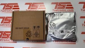
STEP 2. Check label & packaging
1. Compare the label with Depot
- Brand Logo → Arrangement mode
- Label Icon → Label Fonts
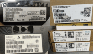
2. Check packaging box and bag seal → whether original factory seal, type on the bag edge
3. Check production date on the reel → Tray packing belt whether is original
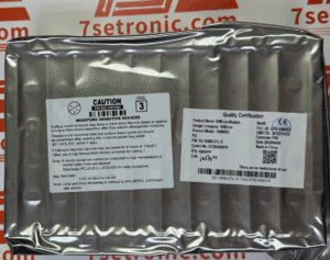
4. Check the tape on the reel is complete or not
- Whether the tape is out of shape.
- Whether the tape is damaged → if the tape is damed. check whether the parts is affected
5. Check the tape edge (circle) of the reel
Whether opposite of the label → if in the same direction → The tape might be upside down
STEP 3. Appearance inspection of parts
1. The chip silkscreen information corresponds to the official website
D/C corresponds with label → logo information right or not → Whether with production place (prevent domestic parts) → Front abd back positioning holes → Compare with original, logo and font
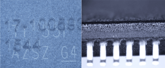
Re-typed recoated
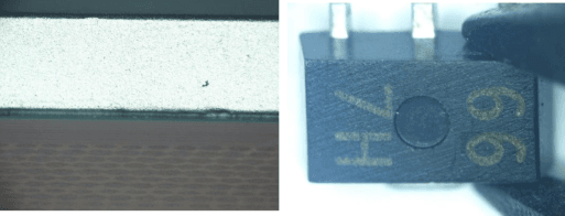
cap replaced sanded
2. Package Dimensions
- Compare with specification and verify packaging
- Use digital display calipersI measure the size of the parts → Note the thickness of the chip

3. Check for oxidation → Inspection the pin under the microscope
- Whether iturn yellow → Whether is corrosion
- Whether the Pin section has copper color → Whether the pin is complete → Whether is reweld, reconnect
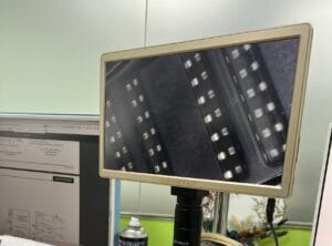
4. Check bead of BGA packaging
Whether is pressed → Whether the bottom plate is stained → Whether tin is available (prevent replanting)
5. Inspection the chip under the micoscope
- Whether the screen printing on the chip surface is clear and complete → Whether there are scratches, notches, dirt.
- If the surface of the chip is flat and rough, no concave-convex smoothness, it is re-polished. The side of the chip with obvious color difference, it is secondary coating, which can be tested with acetone. →Making Permanency Test → Using acetone towipe the surface of the chip, the surface of the chip fade, which is caused by the secondary coating of the chip
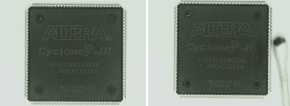
Test before test Test failed.
6. The capacitance and resistance should be measure by bridge tester
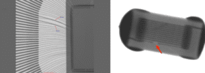
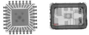
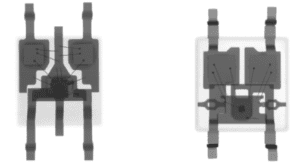
STEP 4. X-Ray Test
- Check the internal crystal and wire structure
- Save the X-Ray images and put into Depot
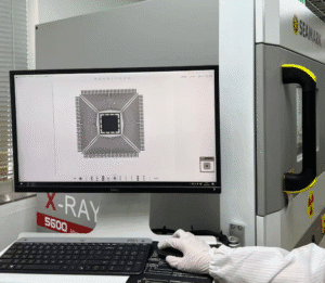
Wire bonding crossed: electrode broken: Bonding/wafer defects: packaging gaps: Structural differences:
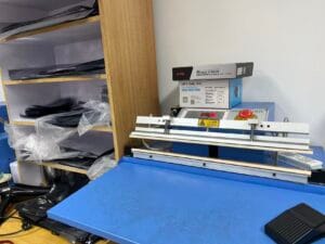
STEP 5. Vacuum Sealing & Storage
- After inspection and testing (QC), repackage qualified components with moisture-proof bags
- Perform vacuum sealing to prevent oxidation and moisture contamination
- Label each bag with inspection date, operator, and batch code
- Store in temperature- and humidity-controlled environment before shipment
